PCB inspection guide - improve quality at every stage of SMT production
Whether you're assembling high-mix, low-volume PCBs or running a fully automated SMT line, one thing remains constant:
every printed circuit board must meet the same quality expectations before it reaches your customer.
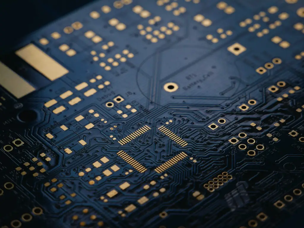
Today's electronics are becoming smaller, faster and more complex. Fine-pitch components, BGAs, 01005 packages and increasingly demanding quality standards leave little room for error. While automated inspection technologies continue to evolve, experienced operators and the right inspection equipment remain essential for identifying defects, verifying workmanship and supporting continuous process improvements.
This PCB inspection guide explains how PCB inspection fits into modern SMT production, where manual and automated inspection complement each other, and how choosing the right inspection methods can help reduce defects, improve first-pass yield and strengthen overall product quality.
Whether you work in an OEM or EMS environment, this guide will provide a practical overview of the PCB inspection process - from incoming inspection to final quality control.

What is PCB inspection?
PCB inspection is the process of examining printed circuit boards throughout manufacturing to ensure they meet design specifications and quality requirements before moving to the next production stage or reaching the end customer.
The goal is not simply to find defects. Effective PCB inspection helps manufacturers identify process deviations early, minimise scrap, reduce costly rework and continuously improve production performance.
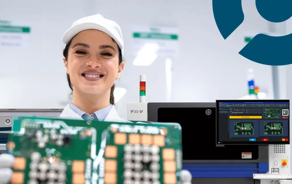
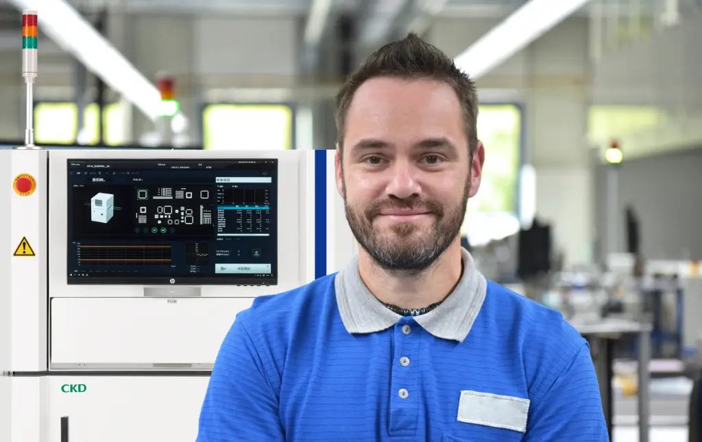
Inspection takes place at several points throughout an SMT assembly process. Depending on the application, it may involve manual visual inspection, digital microscopes, inspection cameras or automated inspection technologies such as SPI, AOI and AXI. Each method contributes valuable information that helps maintain stable production and consistent product quality.
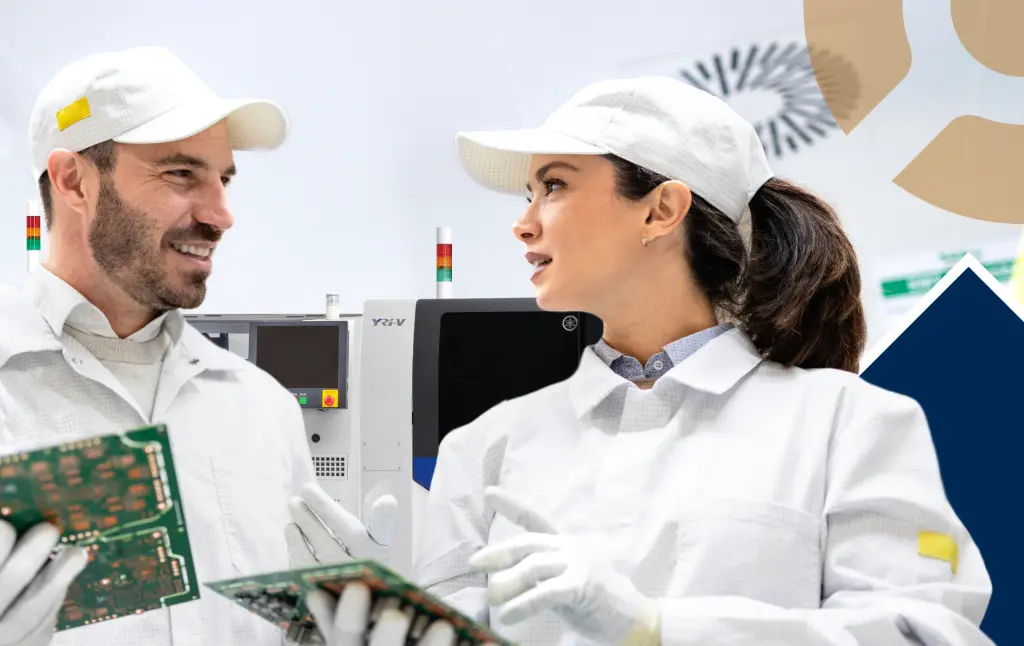
Rather than replacing one another, manual and automated inspection work together. Automated systems deliver speed, repeatability and traceability, while manual inspection allows operators to investigate details, verify uncertain results and perform tasks that still require human judgement.

A well-planned inspection strategy supports more than quality assurance
It also helps manufactures:
Detect defects before they become costly failures
Improve first-pass yield
Reduce rework and production downtime
Support IPC acceptance criteria and customer quality requirements
Create valuable feedback for continuous process optimisation
When inspection becomes part of the manufacturing process - not just the final checkpoint - it helps build a more stable and efficient SMT production environment.
PCB inspection throughout the SMT process
Successful PCB inspection does not happen at a single workstation. Instead, it forms a continuous quality thread throughout the entire SMT assembly process.
Every inspection point answers a different question:
- Is the incoming PCB suitable for production?
- Has solder paste been applied correctly?
- Are components mounted accurately?
- Have solder joints formed correctly?
- Does the finished PCB meet customer requirements?
By identifying issues as early as possible, manufacturers avoid allowing small process deviations to develop into expensive quality problems later in production.
Let's look at where PCB inspection creates the greatest value
Below you find six of the most important board inspections in PCB assembly production
Incoming PCB inspection
Quality starts long before components are placed on the board.
Incoming PCB inspection verifies that bare PCBs meet manufacturing specifications before entering production. Even small imperfections can affect downstream processes, increase rework or reduce product reliability.
Typical inspection points include:
- Surface contamination
- Scratches or mechanical damage
- Warpage
- Copper defects
- Incorrect drill holes
- Damaged solder mask
- Poor silkscreen quality
- PCB dimensional accuracy
Catching these issues before production begins helps prevent unnecessary machine stops, assembly errors and wasted components.
For many manufacturers, incoming inspection also provides valuable supplier feedback. If recurring defects are identified early, suppliers can address quality issues before they impact future deliveries.
PCB inspection after solder paste printing
One of the most important inspection stages takes place immediately after solder paste printing
The quality of every solder joint begins with the solder paste deposit. If the paste volume or position is incorrect, later processes cannot fully compensate for the error.
Typical defects include:
- Insufficient solder paste
- Excess solder paste
- Misaligned deposits
- Bridging between pads
- Missing paste
- Smearing
Many SMT manufacturers use Solder Paste Inspection (SPI) systems to measure solder paste volume, height and position automatically. By identifying printing deviations early, production teams can adjust stencil printing before defects appear further down the line.
Even in highly automated production, manual inspection remains valuable when verifying process changes, investigating new product introductions or confirming unusual SPI results.
This early inspection stage often has one of the greatest impacts on improving first-pass yield throughout the entire SMT process.
PCB inspection during component placement and reflow
As components become smaller and PCB layouts more densely populated, visual inspection alone is rarely enough to guarantee consistent quality. After solder paste printing, every stage of the SMT process presents new opportunities for defects to occur, making systematic AOI inspection essential.
During component placement, manufacturers want to confirm that each component has been picked, oriented and positioned correctly before reflow soldering takes place. While modern pick & place machines achieve extremely high placement accuracy, factors such as feeder issues, incorrect component data or damaged components can still affect the result.
Once the PCB passes through the reflow oven, attention shifts from component placement to solder joint quality. This is where the majority of electrical and mechanical connections are formed, and where many defects become visible.
Common defects identified during PCB inspection include:
- Tombstoned components
- Component misalignment
- Solder bridges
- Insufficient solder joints
- Cold solder joints
- Lifted leads
- Missing components
- Incorrect polarity
- Damaged components
- Excess solder residue
Finding these defects early prevents faulty boards from progressing further through production, where repairs become more time-consuming and expensive.
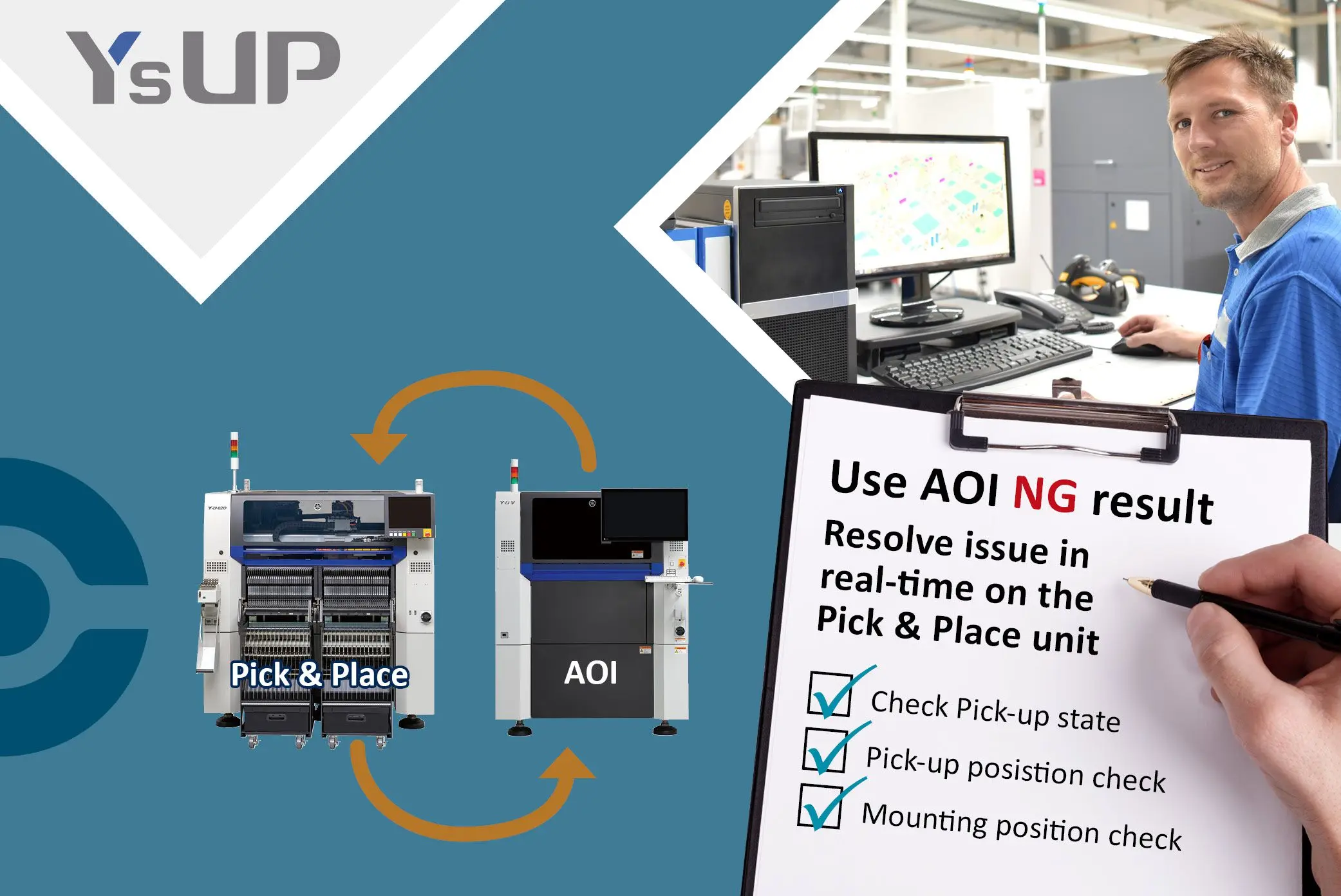
For high-volume production, many manufacturers rely on Automated Optical Inspection (AOI) to inspect every assembled PCB with consistent speed and repeatability. AOI compares the assembled board against predefined inspection criteria, helping detect placement errors and soldering defects that may otherwise go unnoticed.
However, even the most advanced AOI system is not designed to replace every manual inspection task.
When engineering teams introduce a new PCB, optimise production parameters or investigate process deviations, experienced operators often perform manual verification alongside automated inspection. This combination provides confidence in both the inspection results and the production process itself.
Manual PCB inspection vs automated inspection

An a world with more AI and inspection automation is a common misconception is that manual PCB inspection becomes unnecessary once AOI, SPI or AXI systems are installed.
In reality, successful SMT manufacturers combine both approaches because each offers unique advantages.
Automated inspection technologies excel at inspecting large production volumes consistently. They provide objective measurements, improve traceability and reduce inspection time, making them ideal for repetitive production.
Manual PCB inspection, on the other hand, gives operators the flexibility to investigate complex assemblies, evaluate unusual defects and support engineering decisions that require human judgement.
The most effective inspection strategies combine both methods.
Manual PCB inspection | Automated PCB inspection |
Flexible for prototypes and NPI | High-speed inspection of production volumes |
Ideal for PCB rework | Consistent inspection criteria |
Excellent for detailed investigations | Automatic documentation and traceability |
Supports process troubleshooting | Detects repetitive defects efficiently |
Operator experience adds valuable judgement | Reduces inspection time and operator workload |
Rather than choosing one over the other, manufacturers achieve the best results by allowing automated systems to perform routine inspections while experienced technicians investigate exceptions and perform detailed quality assessments.
PCB inspection during PCB rework
PCB rework requires a completely different inspection approach than high-speed production.
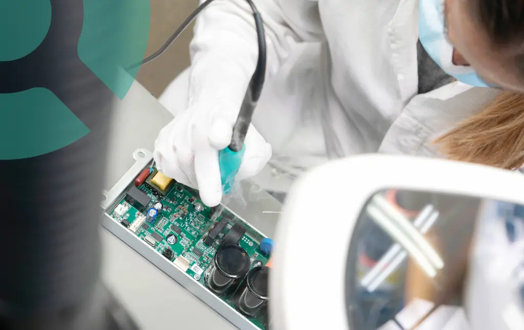
When replacing a BGA, repairing a fine-pitch IC or correcting a solder bridge, technicians need far greater visual detail than an automated inspection system typically provides.
This is where high-quality inspection equipment becomes indispensable.
During PCB rework, technicians often inspect:
- BGA pad condition
- Solder joint quality
- Fine-pitch leads
- Lifted pads
- PCB damage
- Component alignment
- Flux residues after cleaning
- Micro-cracks
- Delicate traces and vias
Accurate inspection before, during and after rework helps ensure that repairs restore the PCB to the required quality standard rather than introducing new defects.
For these tasks, many manufacturers use stereo microscopes or digital inspection microscopes that provide clear magnification, excellent depth perception and ergonomic viewing over extended periods.
Digital inspection systems also make it easier to document repairs, capture images for quality reports and collaborate between production, engineering and quality departments.
In repair environments, inspection is not simply about confirming that a repair has been completed - it is about verifying that the repaired PCB will perform reliably throughout its expected service life.
Final PCB inspection before shipment
The final inspection stage represents the last opportunity to verify product quality before a PCB leaves the factory.
Even when multiple inspection systems are integrated throughout the SMT line, final PCB inspection remains an important safeguard for many manufacturers, particularly within industries where reliability and traceability are critical.
Depending on the application, final inspection may verify:
- Overall workmanship
- Solder joint quality
- Component orientation
- Connector positioning
- Mechanical damage
- Cleanliness
- Labelling and traceability
- Customer-specific acceptance criteria
Some manufacturers perform sample inspections, while others inspect every PCB depending on production requirements and quality standards.

The purpose is not only to identify defects but also to confirm that the entire manufacturing process has produced a PCB ready for installation and long-term operation.
A structured final inspection process gives manufacturers greater confidence before products are delivered to customers and provides valuable feedback for continuous improvement across the production line.
What equipment is used for PCB inspection?
Choosing the right inspection equipment depends on more than magnification or camera resolution. The best solution is determined by the complexity of your PCB assemblies, production volume, inspection requirements and the stage of the SMT process where the equipment will be used.
For many manufacturers, PCB inspection involves a combination of automated inspection systems and manual inspection tools. Each plays a specific role in delivering consistent quality while keeping production efficient.
Let's take a closer look at the most common inspection solutions used throughout modern SMT production.
Inspection microscopes
Inspection microscopes remain one of the most valuable tools in electronics manufacturing.
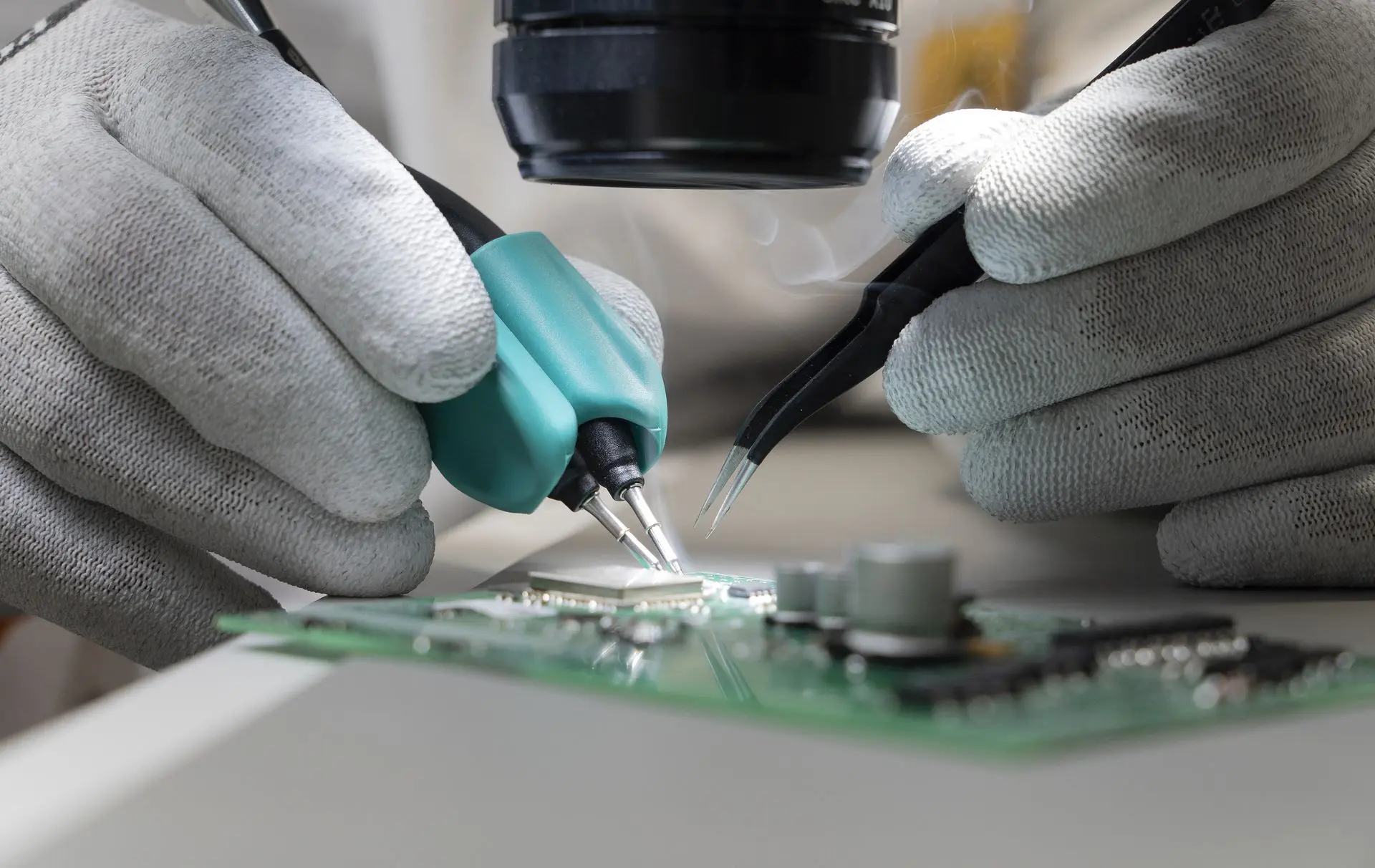
Even in highly automated SMT environments, there are situations where an experienced operator needs to examine a PCB in greater detail. Whether verifying a solder joint, inspecting a BGA landing area or evaluating a delicate repair, a microscope provides the clarity needed to make confident decisions.
Inspection microscopes are commonly used for:
- PCB rework
- Soldering applications
- Failure analysis
- Incoming PCB inspection
- Prototype assembly
- Quality verification
- Training new operators
Stereo microscopes are particularly popular because they provide true depth perception. This makes it easier to position soldering tools accurately and inspect three-dimensional features such as solder fillets, component leads and connector pins.
Comfort is equally important.
Operators may spend several hours each day inspecting assemblies, so ergonomic microscope design can help reduce fatigue while improving inspection consistency.
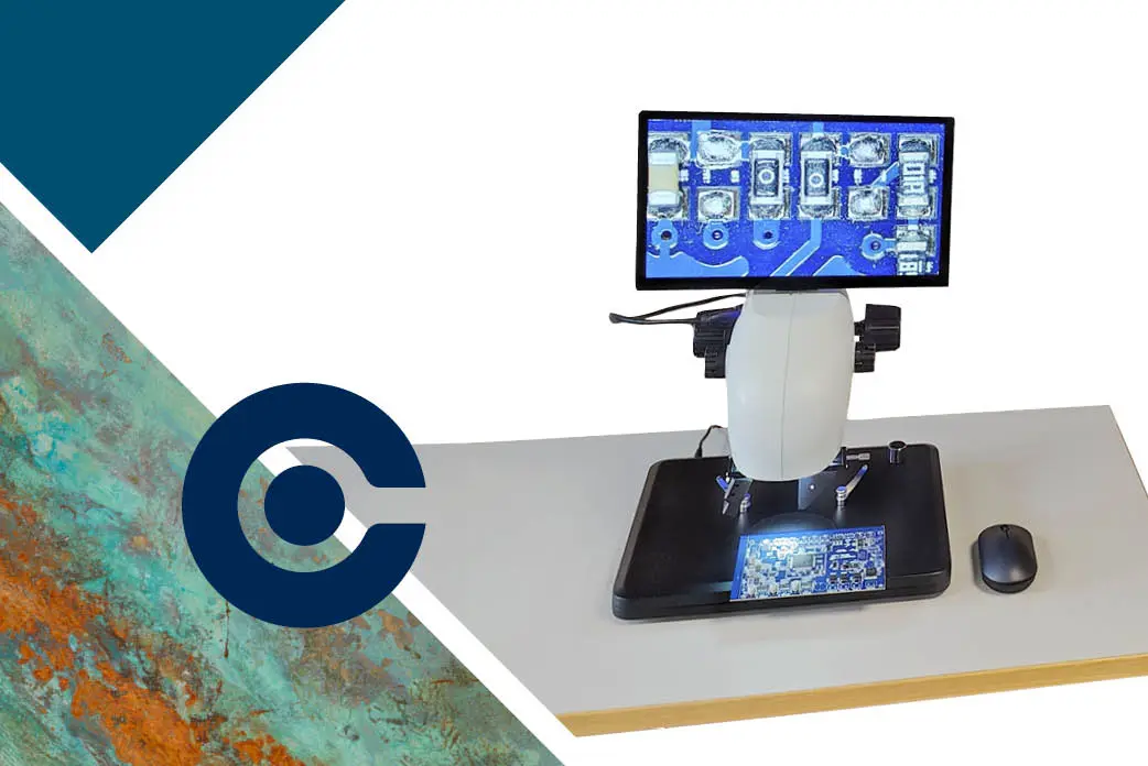
Digital microscopes
Digital microscopes have become increasingly common across both OEM and EMS production environments.
Unlike traditional optical microscopes, digital microscopes display the inspection image on a monitor, allowing multiple people to view the same PCB simultaneously. This is particularly valuable during process optimisation, training sessions, customer audits and quality investigations.
Digital microscopes also make documentation significantly easier.
Images and videos can be captured to:
- Document quality findings
- Support failure analysis
- Create work instructions
- Assist operator training
- Share inspection results across departments
- Support customer communication
For engineering teams working with continuous improvement, being able to compare inspection images over time provides valuable insight into recurring production trends and process stability.
Inspection cameras
Inspection cameras offer another practical solution when magnification requirements are moderate but flexibility and collaboration are important.
Compared with microscopes, inspection cameras often provide a larger field of view, making them useful for inspecting connectors, larger PCB assemblies and mechanical details.
Many manufacturers use inspection cameras for:
- Visual quality checks
- Assembly verification
- Documentation
- Training operators
- Process reviews
- Remote technical support
Displaying inspection images on a larger screen also makes discussions between production, engineering and quality departments much easier, especially when investigating complex defects or introducing new products into production.
Good lighting makes better PCB inspection
Magnification is only part of successful PCB inspection. Without proper lighting, even the highest-quality microscope cannot reveal every detail.
Modern PCB assemblies often include reflective solder joints, densely populated components and fine-pitch packages that create shadows and glare. Adjustable LED lighting helps improve visibility by providing even illumination across the inspection area.
Depending on the application, manufacturers may use:
- Ring lights
- Adjustable LED illumination
- Coaxial lighting
- Directional lighting
- Diffused lighting
Selecting the right lighting solution improves defect visibility while reducing eye strain during extended inspection work.
Many inspection challenges that initially appear to require greater magnification can actually be solved simply by improving the lighting conditions.

How to choose the right PCB inspection solution?
No two SMT production environments are identical.
A manufacturer producing automotive control units has different inspection requirements than an EMS provider assembling high-mix prototypes or a company specialising in aerospace electronics.
When selecting a PCB inspection solution, it is worth considering the complete manufacturing process rather than focusing on a single workstation.
Questions worth asking include:
- What types of PCB assemblies do you manufacture?
- What component sizes are most common?
- How complex are your PCB designs?
- Is production high-volume or high-mix?
- How much PCB rework is performed?
- Do customers require documented inspection results?
- Will the equipment be used for production, engineering or training?
The answers help determine whether a digital microscope, stereo microscope, inspection camera or automated inspection system is the most appropriate solution.
In many cases, manufacturers achieve the greatest value by combining several inspection technologies.
For example, SPI verifies solder paste deposits, AOI inspects assembled PCBs, AXI examines hidden solder joints beneath BGAs, while microscopes support engineering, manual inspection and PCB rework.
Rather than viewing these solutions as competing technologies, they should be considered complementary tools within a complete PCB inspection strategy.
By selecting equipment that matches both today's production needs and tomorrow's manufacturing challenges, companies create a more flexible inspection process that supports long-term quality improvements.
Five tips for better PCB inspection
Whether your production is highly automated or relies on experienced operators, a few practical principles can significantly improve inspection quality and consistency
1. Inspect as early as possible
Finding a defect immediately after solder paste printing is far less expensive than discovering it after final assembly.
Early inspection reduces scrap, shortens troubleshooting time and helps maintain stable production.
2. Standardise inspection criteria
Clear inspection guidelines help ensure every operator evaluates PCBs using the same acceptance criteria.
Consistency improves quality and reduces unnecessary discussions about borderline defects.
3. Use the right inspection tool for the task
Not every inspection requires maximum magnification.
Choosing the appropriate combination of AOI, SPI, AXI, microscopes and inspection cameras helps optimise both inspection speed and inspection quality.
4. Document recurring defects
Capturing images of recurring defects makes it easier to identify trends, improve operator training and optimise manufacturing processes over time.
Small observations often lead to major process improvements.
5. Remember, inspection supports process improvement
The best manufacturers do not view inspection as simply finding faulty boards.
Instead, they use inspection data to improve stencil printing, component placement, soldering processes and overall production stability.
As inspection becomes part of a continuous improvement culture, quality increases while production costs often decrease.
Building a stronger PCB inspection process
Effective PCB inspection is not about finding faults at the end of production - it's about building quality into every stage of the SMT process.
From incoming PCB inspection and solder paste verification to AOI, AXI, manual inspection and PCB rework, each inspection point provides valuable insight into your manufacturing process. Together, these inspection methods help identify deviations early, improve first-pass yield and reduce the cost of defects before products reach your customers.
As PCB assemblies continue to become smaller and more complex, manufacturers are increasingly combining automated inspection systems with high-quality manual inspection equipment. Automated solutions deliver speed, consistency and traceability, while experienced operators provide the flexibility and technical judgement needed for prototypes, process optimisation and complex rework tasks.
The most successful OEM and EMS manufacturers do not view inspection as a separate quality function. Instead, they use inspection data to improve every aspect of production - from stencil printing and component placement to soldering quality and continuous process improvement.
By selecting the right PCB inspection equipment and implementing a structured inspection process, manufacturers can achieve:

- Higher product quality
- Improved first-pass yield
- Fewer production interruptions
- Reduced scrap and rework
- Better traceability
- Greater customer confidence
Whether you're evaluating your first inspection microscope, expanding your inspection capabilities or investing in a complete SMT inspection solution, understanding where and how PCB inspection creates value is the first step towards building a more reliable manufacturing process.

Explore PCB inspection solutions for SMT production
Every SMT production environment has different inspection requirements.
Some manufacturers require a flexible microscope for PCB rework and manual inspection, while others are looking for automated inspection technologies such as SPI, AOI or AXI to support higher production volumes and increased traceability.
At CORE-emt, we help OEM and EMS manufacturers across Scandinavia and the Baltic region identify inspection solutions that match their production requirements - whether you're upgrading a single workstation or developing a complete SMT inspection strategy.
Explore our PCB inspection solutions for SMT lines or other inspection solutions to learn more about inspection equipment for SMT production, or discover how automated and manual inspection can work together to improve product quality throughout your manufacturing process.